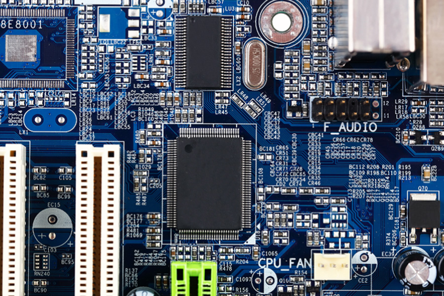
The complexity of modern chip design is staggering. Leading-edge systems-on-chip require billions of transistors, intricate interconnects, and carefully balanced trade-offs in performance, power, and reliability. The cost of designing such chips now exceeds $500 million per project, with timelines stretching over multiple years. This burden has concentrated design capability in the hands of only a few firms able to absorb the expense. New approaches are urgently needed to accelerate cycles and broaden participation. AI-enabled design tools and digital twin simulations offer a path forward. Erik Hosler, a strategist in semiconductor design innovation, underscores that the future of chipmaking will depend on intelligent tools as much as physical fabs. His perspective highlights how smarter design platforms are becoming as critical as manufacturing capacity itself.
AI-driven design is not merely about efficiency, but also about shifting the economics of innovation. By automating tedious tasks, optimizing layouts, and simulating performance virtually, these tools shorten cycles while lowering costs. Digital twins add another layer, providing virtual models of chips and systems that can be tested before fabrication. Together, they promise to change how the semiconductor ecosystem innovates, opening doors for startups, accelerating defense applications, and delivering technologies that reach end users faster.
The Rising Cost of Chip Design
For decades, Moore’s Law provided a predictable cadence of scaling, but design costs have escalated with each new generation. At advanced nodes like 3 nanometers, the expense of masks, verification, and integration now exceeds half a billion dollars for a single design. Only firms with enormous resources, like Apple, Nvidia, or Qualcomm, can consistently deliver at the cutting edge.
This concentration limits competition and slows the pace of innovation. Smaller companies face prohibitive barriers, and even well-capitalized firms must carefully choose which designs to pursue. Meanwhile, long design cycles mean that opportunities can be lost, as market conditions shift faster than chips can be brought to production.
Breaking this cycle requires tools that compress time, reduce costs, and broaden participation. AI and digital twins are emerging as precisely those enablers.
Generative AI in Design
Generative AI is proving to be a powerful ally in chip design. By training on vast datasets of circuit layouts and design rules, AI models can propose optimized architectures, identify bottlenecks, and predict how changes will affect performance.
One major application is in verification. Traditionally, design verification consumes the majority of engineering resources, as teams must test errors across countless edge cases. AI-driven verification automates much of this process, rapidly identifying anomalies and reducing human workload.
Generative AI can also explore design spaces beyond human intuition. By simulating thousands of variations, it uncovers architectures that balance speed, power, and cost in novel ways. It accelerates iteration, reduces errors, and allows teams to focus on higher-level innovation rather than manual tasks. The result is a faster, more efficient design pipeline that lowers barriers for smaller firms while enhancing productivity for established players.
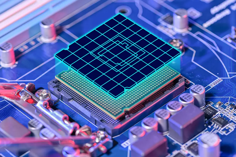
Digital Twins as Virtual Proving Grounds
Digital twins extend the power of AI by creating full-system simulations that replicate chips and devices in virtual environments. Instead of relying solely on physical prototypes, engineers can test performance, reliability, and thermal behavior in silico before fabrication.
For example, a digital twin of a processor can model how it will interact with memory, accelerators, and software in real-world conditions. It allows engineers to test power management strategies, identify thermal bottlenecks, and predict reliability under stress. The insights gained from these simulations reduce the number of costly prototype runs and shorten the time to market.
Digital twins also enable continuous optimization. Once a chip enters production, its twin can be updated with real-world performance data, guiding refinements and informing next-generation designs. This feedback loop ensures that innovation is not a one-off process but an ongoing cycle.
Applications Across the Ecosystem
AI-enabled design tools and digital twins have transformative applications across the semiconductor ecosystem.
Startups:
Smaller companies can enter the market without massive upfront investments, using AI tools to design competitive chips with lean teams.
Defense:
Rapid prototyping with digital twins allows the Department of Defense and contractors to develop secure, custom chips for mission-critical systems without long delays.
Automotive:
Cars require chips that balance performance with safety and reliability. Digital twins can test these conditions virtually, accelerating innovation in autonomous and electric vehicles.
Healthcare:
Medical devices often rely on highly specialized chips. AI tools reduce development time, enabling faster innovation deployment.
These tools democratize innovation by lowering barriers and accelerating design, ensuring that the next wave of semiconductor breakthroughs comes from a diverse group of contributors.
Innovation Requires Smarter Tools
The success of semiconductor innovation ultimately depends on meeting user expectations. Whether in smartphones, servers, or defense systems, end users care about performance, reliability, and experience, not the technical details of how chips are made.
Erik Hosler points out, “They only expect a certain experience with the rollout of a new technology.” His observation underscores the role of AI-enabled design tools and digital twins. By accelerating design cycles and improving accuracy, these tools ensure that users receive the seamless performance they demand, regardless of underlying complexity.
The message is clear: sustaining semiconductor leadership is not just about building bigger fabs. It is about providing smarter tools that allow designers to deliver innovations faster, cheaper, and with greater reliability. AI and digital twins embody this principle, offering pathways to reduce risk and increase competitiveness.
Design Intelligence as a Competitive Edge
The semiconductor industry stands at a crossroads. The cost and complexity of design threaten to slow innovation, but AI-enabled tools and digital twins provide a way forward. By automating tasks, simulating performance, and guiding optimization, they reduce barriers and accelerate cycles.
For the U.S. and its allies, investing in these tools is as important as investing in fabrication. Design intelligence creates a competitive advantage by ensuring that ideas can be turned into products quickly and effectively. It also democratizes innovation, giving startups, universities, and smaller firms a role in shaping the future of compute.
Design intelligence now has a competitive edge. As AI and digital twins reshape design economics, they will define who leads in semiconductors and, by extension, in advanced computing. The nations and companies that master these tools will set the pace of innovation for decades to come.